


 Material Insight: The Dielectric Constant of PCB Materials
 American Made Advocacy: What About the Rest of the Technology Stack?
 It’s Only Common Sense: Great Ideas From John Mitchell’s Book on Hiring Habits
New Technique for Advanced Printed Electronics
March 23, 2016 | AISTEstimated reading time: 5 minutes
For fabrication of organic ferroelectric devices, one of the problems to be solved is to make a homogeneous thin film. The developed printing technique that stimulates thin-film formation from a solution allows formation of highly uniform single-crystalline thin films of organic ferroelectrics. The thin-film device fabricated by the developed technique worked as a memory device with only 3 V which is lower than operation voltage of various memory devices. The developed technique is expected to accelerate the research and development on low power consumption device of printed electronics such as ferroelectric memories and nonvolatile semiconductor FETs.
Details of the results will soon be published online in a German scientific journal, Advanced Materials.
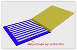
Schematic of fabrication process of single-crystalline thin films of organic ferroelectric molecules
Social Background of Research
Active R&D of the "printed electronics", which applies printing technologies to the production of electronic devices by forming precise, high-quality, metallic and/or semiconducting patterns, has been conducted globally. So far, several printing methods have been enthusiastically developed to fabricate metallic wires and semiconductor layers for transistors, although the development of printing techniques for other types of materials has not been conducted enough. Ferroelectric materials could reduce the power consumption of electronic devices such as ferroelectric memories in IC cards and nonvolatile semiconductor FETs. Therefore, it is required to develop patterning techniques for ferroelectric thin films though printing technologies.
Ferroelectric materials are generally composed of inorganic materials so that it was considered to be difficult to apply a printing process. Although organic ferroelectric polymer materials are applicable to a printing process, their ferroelectric characteristics are inferior to those of inorganic materials. In recent years, research and development of organic ferroelectrics composed of small molecules have advanced. Some new organic materials showing superior characteristics comparable to inorganic ones have been found. Though thin-film formation of these materials is indispensable for making them into devices, it is difficult to form thin films of the materials. Therefore, it was desired to develop a fabrication technique of uniform thin film without any pinholes through a printing process.
Page 1 of 3
Share on:


Suggested Items
Material Insight: The Dielectric Constant of PCB Materials
05/17/2024 | Dr. Preeya Kuray -- Column: Material InsightIn the world of PCB design, miniaturization can be achieved by using low dielectric constant (Dk) materials. Low Dk materials can allow for a reduction in thickness while maintaining a given trace width, leading to lower transmission loss and higher density circuitry.
IPC APEX EXPO: Some Thoughts About Growth
05/16/2024 | Dan Feinberg, I-Connect007After two and a half days of wandering the aisles at IPC APEX EXPO 2024, for the first time, I almost felt like I was exploring CES. There were so many booths and exhibits that I could describe, but I’d like to focus on the growth and huge value of this event, which has expanded well beyond just the growing and impressive exhibit show floor.
The Shaughnessy Report: Unlock Your High-speed Material Constraints
05/15/2024 | Andy Shaughnessy -- Column: The Shaughnessy ReportThe world of PCB materials used to be a fairly simple one. It was divided into two groups: the “traditional” laminates, often called FR-4, and the high-speed laminates developed especially for high-speed PCBs. These were two worlds that usually didn’t collide. But then traditional laminates started getting better, and high-speed designers and design engineers took notice and started to reconsider what FR-4 could be used for.
Breaking High-speed Material Constraints: Design007 Magazine — May 2024
05/14/2024 | I-Connect007 Editorial TeamDo you need specialty materials for your high-speed designs? Maybe not. Improvements in resins mean designers of high-speed boards can sometimes use traditional laminate systems instead of high-speed materials, saving time and money while streamlining the fab process. In the May 2024 issue of Design007 Magazine, our contributors explain how to avoid overconstraining your materials when working with high-speed boards.
Indium Experts to Present at Electronics in Harsh Environments SMTA Conference
05/13/2024 | Indium Corporationndium Corporation Technical Manager for Europe, Africa, and the Middle East, Karthik Vijay, will deliver a technical presentation and Indium Corporation Senior Technologist, Dr. Ronald Lasky, will deliver both a workshop and technical presentation at the Electronics in Harsh Environments SMTA Conference on May 14-16 in Copenhagen, Denmark.